ECE Projects
|
ECE Projects |
Electronic Projects AudioRF
Circuits |
Voltage Doubler Circuit
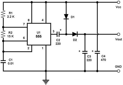
Figure 1. Schematic Diagram for a Voltage Doubling Circuit (capacitor values are in microF) This is a circuit that outputs a voltage Vout that is approximately twice the level of the Vcc voltage. The circuit uses a 555 timer IC configured as an astable multivibrator, i.e., it generates a continuous square wave signal of a set frequency as long as its reset pin (pin 4) is held high. This means that the 555 output toggles between '1' and '0' continuously at the set frequency. When the circuit is powered up and the 555 output (pin 3) goes to logic '1' for the very first time, its near-Vcc voltage level causes C3 to charge up through D2 and also reach near-Vcc level. When the output goes to logic '0', C2 charges from Vcc through D1, also to a near-Vcc level. When the 555 output goes back to logic '1' again, C3 may still have some (if not most) of its charge left, and will allow to charge up to a higher level since it is now effectively in parallel with the series circuit of the 555 level '1' output and the charged C2. After several cycles of C2 and C3 alternately charging, C3 will subsequently build up a voltage level equal to almost twice the Vcc level. This C3 voltage comes from the charge pumped in by the sum of the C2 voltage (near-Vcc) and the 555 output voltage when it is at logic '1' (also near-Vcc). At this point, the output Vout of the circuit will already be almost twice the Vcc level. |
|